Introduction
The Pokemon Go Plus (PGP) is a wearable Dialog Semiconductor DA14580 wristband. It utilizes Bluetooth Low Energy (BLE) to connect to your mobile phone and interact with Pokemon Go. It has a simple interface of merely one push-button switch that allows the player to catch Pokemon and spin Pokestops. In other words, this device allows you to play the mobile game without looking at your phone! When Nintendo first announced the PGP, hacker enthusiasts wanted to create a Do-It-Yourself version. They scouted for any information about the device on the internet and in Pokemon GO Android APK files. Most of the earliest findings were aggregated on Hackaday. After the PGP's official release, efforts to duplicate it were halted due to cryptographic algorithms that verified the device's legitimacy.
A few years ago, Reddit user BobThePidgeon_ wrote a detailed post showing his findings on this "Certification Process". Although very informative, the Pokemon Go development community was still unable to fully replicate the certification process which led to a dry spell for a couple of years. About 11 months ago, Yohanes from Tinyhack.com did the impossible and cracked the complete certification algorithm. Unfortunately, this led to another roadblock; the certification process requires a device's Bluetooth address, a 16 byte device key, and a 256 byte blob key, all embedded in the device's One-Time-Programmable (OTP) memory. The device and blob keys thusfar have been impossible to obtain unless you interface with the SPI chip via soldering.
My Reverse Engineering skills were limited, so I opted to wait for more experienced engineers to report their findings and study them. Yohanes' had an idea for extracting the device/blob keys over-the-air. Needless to say I was inspired to step up to the plate and contribute to the movement! I bought a DA14580 development board, downloaded sample firmware, and began working on this project. I dedicated more than 10 months of my spare time to this project and learned a tremendous amount about embedded devices and BLE in the process.
Prerequisites
Before reading this article, I highly recommend reading these posts for context:
Pokémon Go Plus reverse engineering write up
Reverse Engineering Pokémon GO Plus
Reverse Engineering Pokémon GO Plus Part 2: OTA Signature Bypass
Architectural Layout
I would like to begin by explaining the architecture of the Pokémon Go Plus in great detail. Most of my findings are consistent with /u/_BobThePidgeon's post, which suggests that a counterfeit Pokémon Go Plus uses the same firmware as a real one.
SPI Flash Layout
| Address | Size (bytes) | Name |
|---|---|---|
| 0x00000 | 24688 | Bank 0 - SUOTA Image |
| 0x08000 | 32048 | Bank 1 - PGP Image |
| 0x10000 | 32048 | Bank 2 - PGP Image |
| 0x18000 | 3 | Unknown |
| 0x1E000 | 58 | PGP Bonding Information |
| 0x1F000 | 12 | Product Header |
Figure 1: SPI Flash Layout
During my research, I was able to find out the following:
- The bootloader is stored in OTP.
- The bootloader only attempts to load from Bank 1 and 2.
- Bank 0 contains the SUOTA image. When you write 0x01 to attribute 21c50462-67cb-63a3-5c4c-82b5b9939aef (FW_UPDATE_REQUEST), this image is loaded into memory and executed.
- Bank 1 and Bank 2 are almost exact mirrors of one another. The only difference is the Image ID, which is 0x01 on Bank 1 and 0x00 on Bank 2. This redundancy is necessary in the event that one of the images become corrupted.
- PGP bonding information is saved in section 0x1E000. Although I am not sure what specific information this section contains, I do know that it holds unique information related to your mobile phone. This is evident by the fact the Pokemon Go Plus requires a hard reset in order to connect to other mobile phones. After a hard reset, almost every byte in this section are set to 0x00 as shown in Figure 2.
- The product header contains pointers to Bank 1 and 2 for the bootloader to use and serves no other purpose.
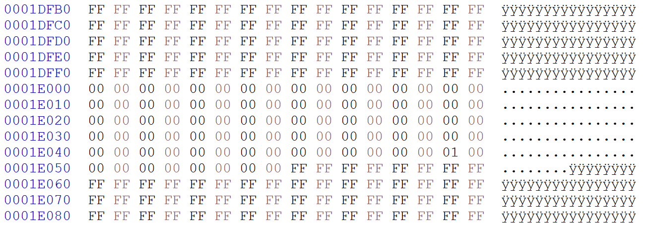
Figure 2: SPI Flash View after hard resetting a Pokémon GO Plus
Image Header
Every image contains an image header.

Figure 3: Sample Image Header
| Field | Size (bytes) | Offset |
|---|---|---|
| Signature (0x7051) | 2 | 0x00 |
| Valid Flag | 1 | 0x02 |
| Image ID | 1 | 0x03 |
| Image Size | 4 | 0x04 |
| Image CRC | 4 | 0x08 |
| Image Version | 16 | 0x0C |
| Timestamp | 4 | 0x1C |
| Encryption Flag | 1 | 0x20 |
| Reserved | 31 | 0x21 |
Figure 4: Image Header fields
Some interesting tidbits about the image header fields:
- The signature must be 0x7051 otherwise the image will fail to load.
- The valid flag must be set to 0xAA, otherwise the bootloader will ignore this image.
- The bootloader uses the image id to determine which image is the latest copy. The bank with the highest image id gets loaded. In the Pokemon Go Plus, Bank 1 is always loaded since it's image id is set to 0x01 and Bank 2 is set to 0x00.
- The image size is used by the bootloader when loading the image. It is also used in SUOTA to let the device know how many bytes to expect from the client.
- The bootloader validates the integrity of the image by computing the CRC and comparing it to the Image CRC. If encrypted, the bootloader decrypts the image before performing the CRC routine.
- The Image Version is a string that contains the firmware version. The bootloader does not use this string. The firmware version in the Pokemon Go Plus is 3.900.1.115r1.
- The Timestamp is the epoch time that the firmware was built. The Pokemon Go Plus firmware was built on 05/28/2015 @ 9:00am UTC.
- The encryption flag determines if the contents of the image are encrypted (minus the image header which is never encrypted). On the Pokemon Go Plus this flag is set only on Bank 1 and 2.
Boot Summary
On system boot, the bootloader loads the product header to find the starting address of the two banks. It then verifies that the bank signature is 0x70 0x51 and that the valid flag is set to 0xAA. If both images are valid, it searches for the most recent image by comparing Image IDs. If the CRC of the latest image is valid, the software is loaded into memory and executed. These requirements are vital to ensuring that a custom firmware will boot on a Pokemon Go Plus.
OTP
The OTP address space is 0x40000 – 0x47FFF.
In order to read the OTP memory, you need to enable reading via CLK_AMBA_REG and OTPC_MODE_REG
inline void enable_read_otp()
{
    // Enable OTP clock
    SetBits16(CLK_AMBA_REG, OTP_ENABLE, 1);
    while ((GetWord16(ANA_STATUS_REG) & LDO_OTP_OK) != LDO_OTP_OK)
    // Set OTP in read mode
    SetWord32(OTPC_MODE_REG, OTPC_MODE_MREAD);
}
After setting OTP to read mode, you can easily read the key and the blob from the pointer
void init_blob()
{
    uint8_t *blob = (uint8_t *)0x47000;
    enable_read_otp();
    memcpy(my_blob, blob, 256);
    disable_read_otp();
}

void init_key()
{
    uint8_t *key = (uint8_t *)0x47120;
    enable_read_otp();
    memcpy(my_key, key, 16);
    disable_read_otp();
}
SUOTA
Software Update Over The Air Update (SUOTA) is a proprietary service created by Dialog Semiconductor. The Service ID is 0xFEF5 and uses the following proprietary BLE characteristics.
SUOTA Characteristics
| Name | UUID | Permissions | Size (bytes) |
|---|---|---|---|
| SPOTA_MEM_DEV | 8082caa8-41a6-4021-91c6-56f9b954cc34 | READ, WRITE | 4 |
| SPOTA_GPIO_MAP | 724249f0-5ec3-4b5f-8804-42345af08651 | READ, WRITE | 4 |
| SPOTA_MEM_INFO | 6c53db25-47a1-45fe-a022-7c92fb334fd4 | READ | 4 |
| SPOTA_PATCH_LEN | 9d84b9a3-000c-49d8-9183-855b673fda31 | READ, WRITE | 2 |
| SPOTA_PATCH_DATA | 457871e8-d516-4ca1-9116-57d0b17b9cb2 | READ, WRITE, WRITE NO RESPONSE | 20 |
| SPOTA_SERV_STATUS | 5f78df94-798c-46f5-990a-b3eb6a065c88 | NOTIFY, READ | 1 |
Figure 5: SUOTA Characteristics
- SPOTA_MEM_DEV is used to send a SUOTA command. The high order byte is the opcode and the remaining 3 bytes can be all zeros, an address, or a memory bank. (Figure 6). The PGP only supports SPOTAR_IMG_SPI_FLASH (and the 0xFX commands). Later I will explain how this characteristic can be exploited to write to any address in SPI flash.
- SPOTA_GPIO_MAP is used to define the GPIO ports to use. On the PGP, this characteristic should be set to 0x05060300
- SPOTA_MEM_INFO is used to read the memory info. The two high order bytes are the number of patches and the two low order bytes is the entire length.
- SPOTA_PATCH_LEN defines the block size.
- SPOTA_PATCH_DATA is used for the client to send the patch data to the device.
- SPOTA_SERV_STATUS is used to notify the client of the service status. (Figure 7)
| Opcode | Value | Operands | Description |
|---|---|---|---|
| SPOTAR_MEM_INT_SYSRAM | 0x00 | 0x000000 - 0xFFFFFF | Send a patch to SYSRAM |
| SPOTAR_MEM_INT_RETRAM | 0x01 | 0x000000 - 0xFFFFFF | Send a patch to Retention RAM |
| SPOTAR_MEM_I2C_EEPROM | 0x02 | 0x000001 - 0x000002 | Send a patch to i2c EEPROM |
| SPOTAR_MEM_SPI_FLASH | 0x03 | 0x000001 - 0x000002 | Send a patch to SPI flash |
| SPOTAR_IMG_INT_SYSRAM | 0x10 | 0x000000 - 0xFFFFFF | Send an image to SYSRAM |
| SPOTAR_IMG_INT_RETRAM | 0x11 | 0x000000 - 0xFFFFFF | Send an image to Retention RAM |
| SPOTAR_IMG_I2C_EEPROM | 0x12 | 0x000001 - 0x000002 | Send an image to i2c EEPROM |
| SPOTAR_IMG_SPI_FLASH | 0x13 | 0x000001 - 0x000002 | Send an image to SPI flash |
| SPOTAR_REBOOT | 0xFD | 0x000000 | Reboot the device. |
| SPOTAR_IMG_END | 0xFE | 0x000000 | The client sends this after sending the image and CRC. Explained in the SUOTA Process. |
| SPOTAR_MEM_SERVICE_EXIT | 0xFF | 0x000000 | Critical error occured on the client, exit SUOTA. |
Figure 6: SPOTA_MEM_DEV commands
| Name | Value | Description |
|---|---|---|
| SPOTAR_SRV_STARTED | 0x01 | Valid memory device configured. Service started. |
| SPOTAR_CMP_OK | 0x02 | SUOTA was successful |
| SPOTAR_SRV_EXIT | 0x03 | SUOTA was forced to exit |
| SPOTAR_CRC_ERR | 0x04 | CRC Error |
| SPOTAR_PATCH_LEN_ERR | 0x05 | The patch received was not equal to the SPOTA_PATCH_LEN characteristic value |
| SPOTAR_EXT_MEM_WRITE_ERR | 0x06 | External Memory Error (Writing to external device failed) |
| SPOTAR_INT_MEM_ERR | 0x07 | Internal Memory Error (Not enough space) |
| SPOTAR_INVAL_MEM_TYPE | 0x08 | Invalid Memory Device |
| SPOTAR_APP_ERROR | 0x09 | Application Error. |
| SPOTAR_IMG_STARTED | 0x10 | SUOTA Started |
| SPOTAR_INVAL_IMG_BANK | 0x11 | Invalid Image Bank selected |
| SPOTAR_INVAL_IMG_HDR | 0x12 | Invalid Image header |
| SPOTAR_INVAL_IMG_SIZE | 0x13 | Invalid Image size |
| SPOTAR_INVAL_PRODUCT_HDR | 0x14 | Invalid Product Header |
| SPOTAR_SAME_IMG_ERR | 0x15 | Same Image error |
| SPOTAR_EXT_MEM_READ_ERR | 0x16 | External Memory Error (Unable to read from external memory) |
Figure 7: SPOTA_SERV_STATUS values
Blocks and Chunks
In order to send an image using BLE, it must be cut down into smaller pieces. Dialog Semiconductor solves this by breaking down the image into a finite number of blocks n, which are then broken down further into a finite number of chunks m (Figure 8). The block size b is set by the client with some limitations. The minimum allowed block size is 64 bytes, any smaller and SUOTA will fail because the device did not receive the entire image header in a single block. Setting the block size to a small number will also force the device to process more blocks, which slows down the overall process. The Official Dialog SUOTA app sets the default block size to 240 bytes and this has worked well enough for me.
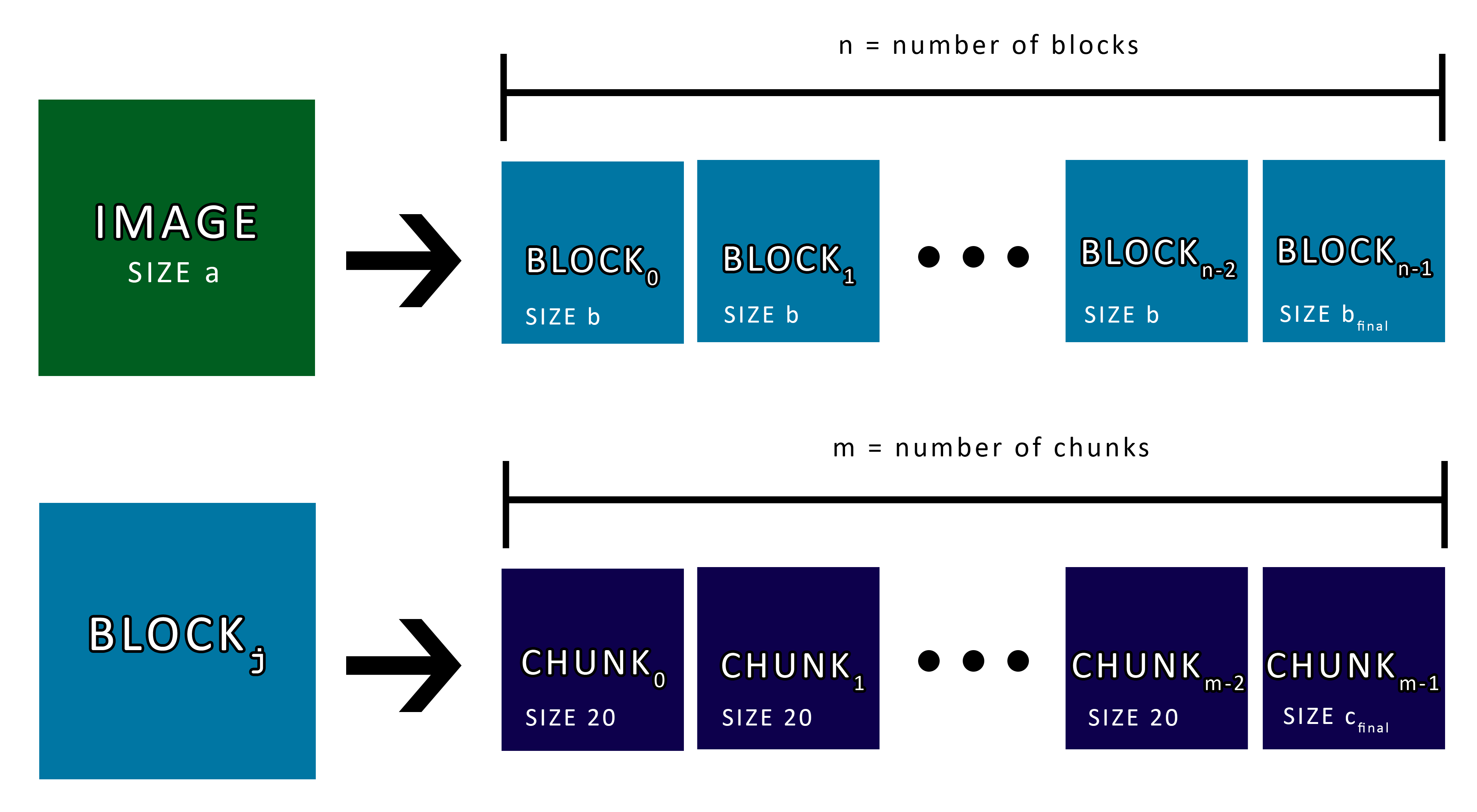
Figure 8: SUOTA Diagram
The number of blocks are computed as follows:
n = a / b + (a % b != 0) ? 1 : 0
The final block length bfinal is computed as follows
bfinal = (a % b != 0) ? (a % b) : b
The chunk size is set to 20 bytes. This is synonymous with the SPOTA_PATCH_DATA characteristic which is 20 bytes in size.
Similarly, the number of chunks in a block are computed as:
m = b / 20 + (b % 20 != 0) ? 1 : 0
The final chunk length cfinal is computed as follows
cfinal = (b % 20 != 0) ? (b % 20) : 20
SUOTA CRC
During SUOTA, a CRC is calculated to verify the integrity of the data sent. This check applies to SUOTA only and should not be confused with the image header CRC. Both the client and DA14580 will calculate their own CRC from the patch data. If they match then integrity is verified, otherwise SPOTA_SERV_STATUS will NOTIFY a SPOTAR_CRC_ERR.
The CRC calculation works as follows:
unsigned char calculate_crc(unsigned char image[], int size)
{
    unsigned char crc = 0;
    for (int i = 0; i < size; i++)
    {
        crc ^= image[i];
    }
    return crc;
}
SUOTA Process
The following is the steps required to update a PGP with a new image.
- Connect the PGP to the Pokemon Go app.
- Write 0x01 to characteristic FW_UPDATE_REQUEST. The PGP will automatically disconnect then run Bank 0.
- Reconnect to the PGP, these SUOTA characteristics should now be visible.
- Register to SPOTA_SERV_STATUS to know if any errors occur.
- Write 0x13000001 (SPOTAR_IMG_SPI_FLASH << 24 | 0x01) to SPOTA_MEM_DEV.
- Wait for SPOTA_SERV_STATUS to NOTIFY SPOTAR_IMG_STARTED.
- Write 0x05060300 to SPOTA_GPIO_MAP.
- Write the block length b to SPOTA_PATCH_LEN
- Begin writing the chunks one at a time to SPOTA_PATCH_DATA.
- If the final block length bfinal is less than b, write bfinal to SPOTA_PATCH_LEN
- Write the chunks of the final block to SPOTA_PATCH_DATA
- Write 0x0001 to SPOTA_PATCH_LEN
- Write the 1 byte CRC to SPOTA_PATCH_DATA
- Write 0xFE000000 (SPOTAR_IMG_END << 24) to SPOTA_MEM_DEV.
- The DA14580 will verify the CRC. If correct, the DA14580 will set the valid flag to 0xAA and the client will receive SPOTAR_CMP_OK from SPOTA_SERV_STATUS. The new firmware will be loaded on restart.
The process seems simple enough, but implementing SUOTA is half the battle. I tried updating Bank 1 using the official Dialog Semiconductor SUOTA App and was greeted with this lovely error.
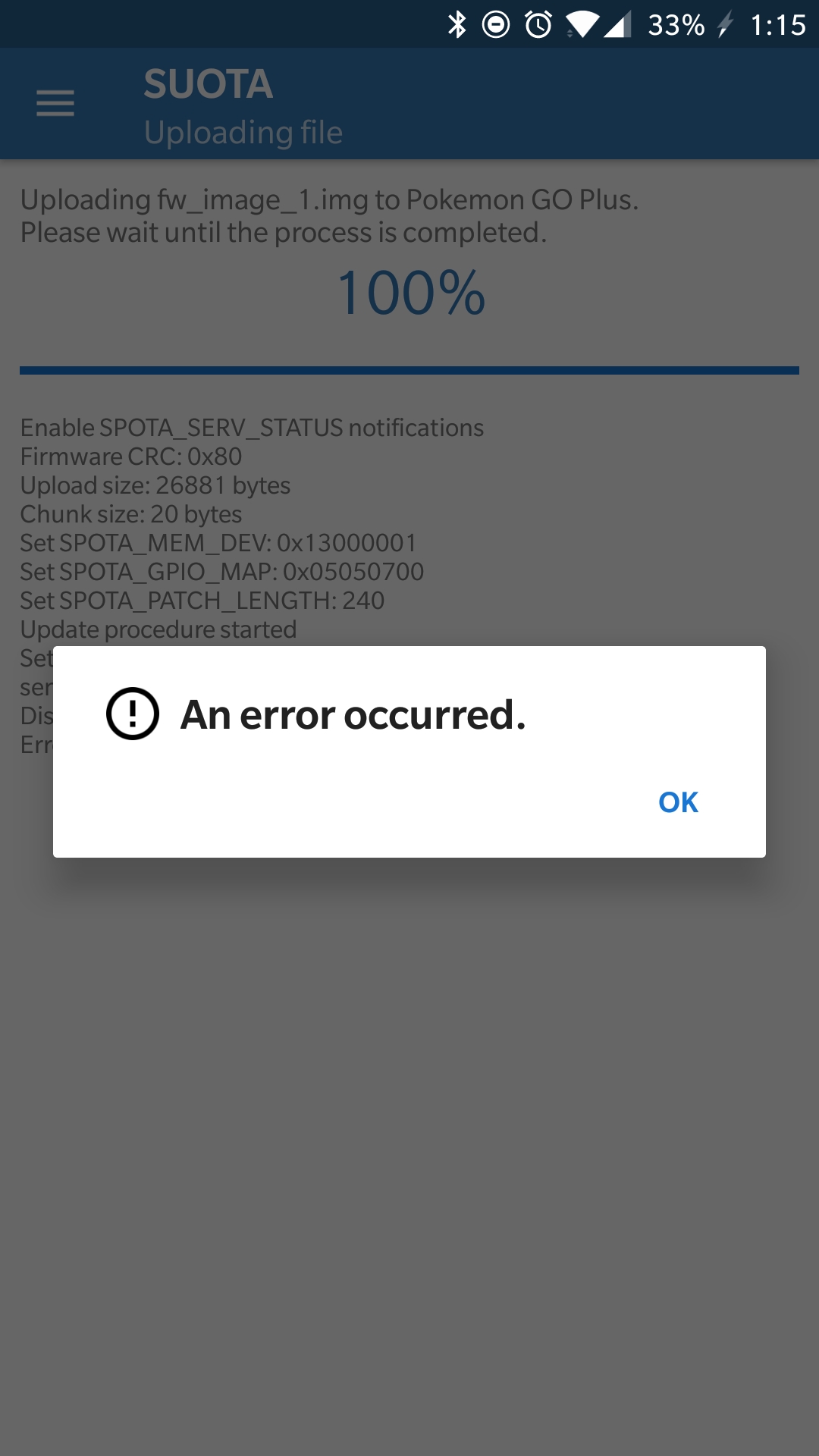
Figure 9: Suota error when using an official client.
SPOTA_SERV_STATUS returned an error code 23 which does not exist in the DA14580 SDK! I immediately suspected that there was some sort of check to verify that the new image came from Nintendo.
Implemention
At this point I will steer away from technical documentation and write about my development experiences.
DA14580 Research
Before I could develop for the DA14580, I needed to learn everything about it. I spent a month researching every technical document available on Dialog Semiconductor's website. The DA14580 Datasheet, AN-B-10 DA1458x using SUOTA, and the UM-B-011 Memory map & scatter file proved to be the most valuable sources of information. The Dialog Semiconductor Staff were most helpful in clarifying any questions that I had about their product. As soon as I was comfortable with the documention I moved on to reading the example source code, which contained a wealth of information that is not readily available in the documentation. All of my significant findings are documented in the previous section.
Interfacing with the SPI Flash
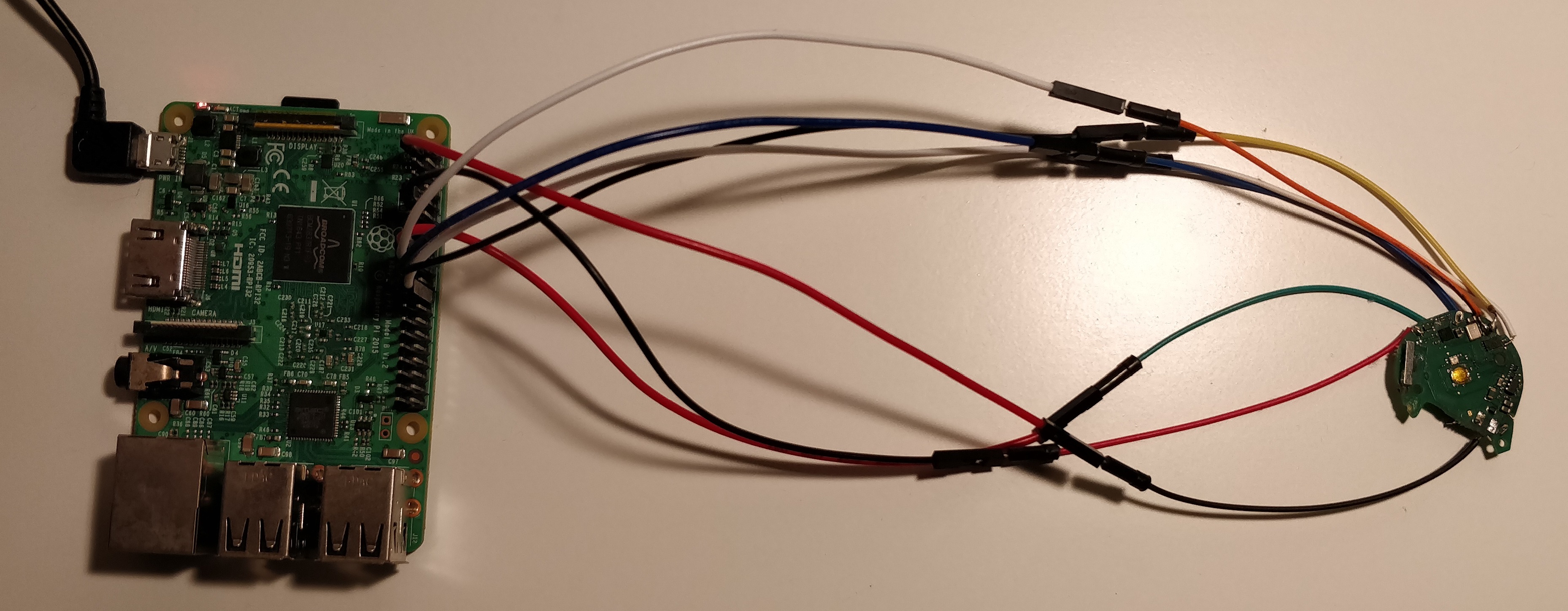
Once I had the technical knowledge, I wanted to interface with the PGP SPI flash in order to see it's contents and to backup the firmware in the event I brick the PGP (which happened more than once!!). This was hands down one of the most difficult steps due to serious hand tremors while soldering. In hindsight, I probably should've eased off the energy drinks before attempting to solder! I used Yohanes' and _BobThePidgeon's posts to find the location of the pins and after careful soldering I managed to interface my PGP with a Raspberry Pi.
Building the Firmware
Creating a custom firmware for the DA14580 is surprisingly easy. The DA14580 SDK provides the framework and numerous sample projects to help you get started. The project file (*.uvprojx) on every sample can be opened and built using Keil uVision IDE. If you are interested in embedded programming, Keil has fantastic support for many microprocessors in the market and is free to use for projects smaller than 32K (thankfully my firmware is 20KB!). There are numerous sample projects in the DA14580 SDK which demonstrate the SoC's capabilities, however I didn't need many of these features. I opted to use ble_app_peripheral, which was the most lightweight sample project that had a custom BLE server already defined (located in user_custs1_def.h/c). I modified this server to define my own PGP key reading characteristics. Since I had a WRITE characteristic, I also had to add a handler in user_catch_rest_hndl() located in user_peripheral.c.
void user_catch_rest_hndl(ke_msg_id_t const msgid,
                          void const *param,
                          ke_task_id_t const dest_id,
                          ke_task_id_t const src_id)
{
  switch (msgid)
  {
      case CUSTS1_VAL_WRITE_IND:
      {
          struct custs1_val_write_ind const *msg_param;
          msg_param = (struct custs1_val_write_ind const *)(param);

          switch (msg_param->handle)
          {
              case CUST1_IDX_RESTORE_VAL:
              {
                  restore_hndler(msgid, msg_param, dest_id, src_id);
              } break;
          }
      } break;
// Rest of the function ...
Note: I'm not a big fan of curly braces around a case statement but I was forced to follow the DA14580 SDK coding style. Don't flame me!
After repeated testing on the DA14580 development board I felt ready to run it on the real thing. I took the ble_app_peripheral_580.hex file that Keil generated and feed it into DA1458x_SUOTA_Multipart_Binary_Generator, which generates a SUOTA image and a flashable binary. (Note: Before you build you need to enable encryption and set the Key/IV in project_multipart_binary_v2.py. The Key and IV are available on Yohanes' Github) I began testing my firmware on the PGP by flashing the SPI chip to confirm that the image was working as intended, after much trial and error I was able to finally read the device and blob key!
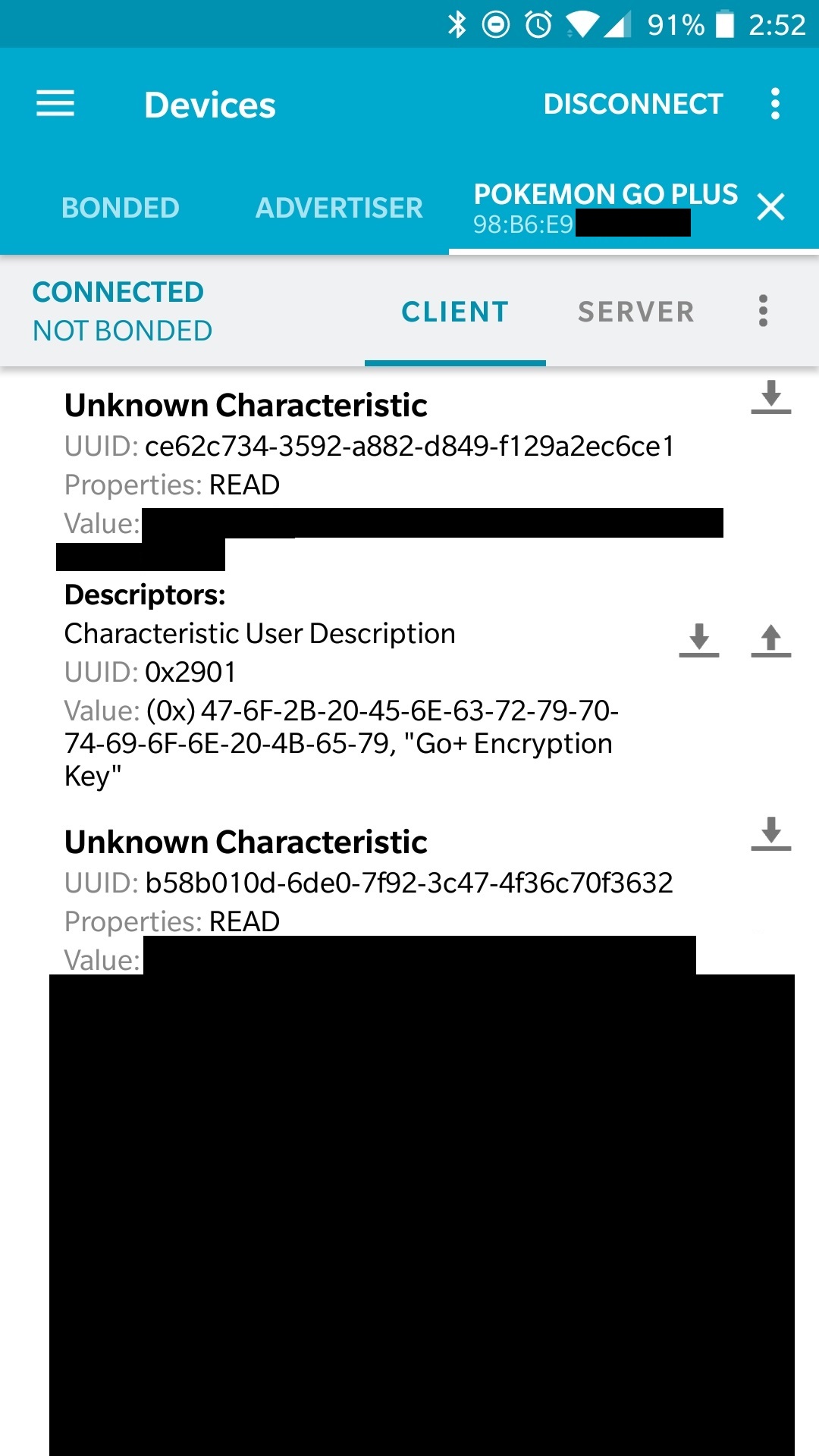
Figure 10: Reading the device and blob key using Nordic Semiconductor nRF Connect (censoring sensative info to prevent my device from being banned)
My custom firmware consists of 4 characteristics
| Name | UUID | Permissions | Size (bytes) |
|---|---|---|---|
| Device Key | 870d5ab1-20bd-b88a-5746-a97f5c33ea58 | READ | 16 |
| Blob Key | fe0002af-f8e3-f1b2-b141-b40adf381d18 | READ | 256 |
| Restore Device | 6b64be6f-5467-d8b5-7143-1716be1b96be | WRITE NO RESPONSE | 1 |
| Restore Device Status | a258f13e-9559-a498-b144-d863a013db06 | READ, NOTIFY | 1 |
After reading the Device and Blob key from its respective characteristic, you can restore the device to it's original state by writing 0x01 to Restore Device. If successful, Restore Device Status will send 0x01 to inform the client that the operation was a success. The client is then free to disconnect and the device will automatically reboot. A negative value from this characteristic means that there was a problem reading from or writing to SPI flash. An error during restoration could brick your device, so extreme caution is advised!
Having a working firmware was a great first step, but the next hurdle was figuring out how to install my firmware on a PGP using SUOTA which would remove the need to interface with the SPI chip directly.
Building the Android Client
Although I have some Android Studio experience under my belt, there's something exceptionally frustrating about Android BLE programming. I also have experience working with WPF, MVVM, and Prism so I figured it would be really cool to try out Xamarin Forms. I was very impressed with the amount of Android support that Xamarin had. There are nuget libraries that make Android permissions, BLE, and toast notifications easy to implement and configure. There were some bizarre bugs such as debugging sessions not starting until I restarted my phone, but overall my experience with Xamarin Form was very positive!
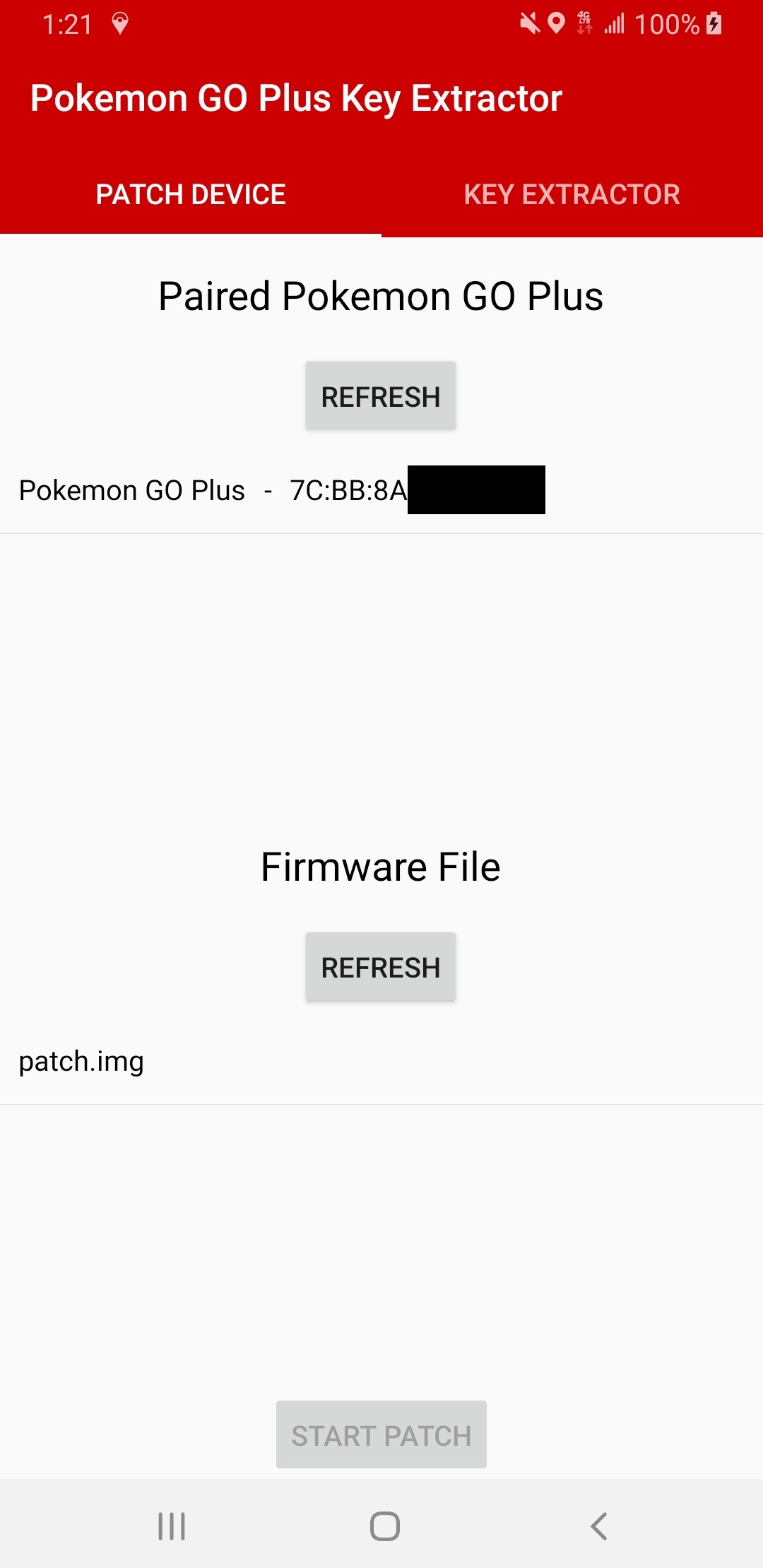
Figure 11: Custom SUOTA Client
The client can perform SUOTA, patch the valid flag (explained in the next section), read the device/blob key, and send the command to restore the original firmware. The Bluetooth address and device/blob key can be saved as a JSON file on your device storage.
Unforunately I do not own an Apple device so I was unable to build an iOS version. If anyone is interested in doing so, feel free to submit a pull request or build your own and I will link it on this post.
Bypassing The Integrity Check
Reverse Engineering the SUOTA Image
One of my favorite tasks in this project was Reverse Engineering (RE) the SUOTA image. As explained in the SUOTA Process section, I needed to understand what caused SPOTA_SERV_STATUS Error 23 and if it was possible to somehow bypass it. I had very little exposure to ARMv6-m assembly so I spent a few weeks preparing by reading the ARM Cortex-M0 Technical Reference Manual. I decided the best point of entry would be to perform static analysis, mainly because I had some previous experience REing x86 software using this method. The DA14580 SDK helped me understand the program flow and removed some of the guess work. Many of the source files in this SDK proved to be an invaluable reference by allowing me to compare assembly instructions with its C code equivalent. boot_vectors.s helped me understand the vector table and application's entry point. rom_symdef.txt helped me understand many low level subroutine calls that were not present in the firmware (they were located in the reserved areas of memory). Each subroutine encountered was a part of a puzzle used to piece together the complete firmware. Eventually I discovered the holy grail, the subroutine app_spotar_read_mem(). This function initializes the SPOTA receiver and most importantly, set the Valid Flag to 0xAA. As I began to reverse subroutine, it became very clear that I was opening a can of worms.
case SPOTAR_IMG_END:
{
    // Client requested to exit service.
    // Calculate CRC
    if (spota_state.crc_calc != 0)
    {
        spotar_send_status_update_req((uint8_t) SPOTAR_CRC_ERR);
    }
    else
    {
        // The Nintendo signature verification is performed here.
        uint8_t result = foobar();
        if (result == 0)
        {
            // Set the Valid Flag to 0xAA
            uint8_t ret = app_set_image_valid_flag();
            spotar_send_status_update_req((uint8_t) ret);
        }
        else
        {
            // Send the error (in my case error 23)
            spotar_send_status_update_req((uint8_t)result);
        }
    }
    app_spotar_stop();
    app_spotar_reset();
    break;
}
Nintendo has a very sophisticated integrity check. The more I dove into foobar, the more I realized I had no idea what was going on anymore!
It was around this time that Yohanes reached out to me, he was on holiday and was offering to help. I enthusiastically accepted his offer and got him up to speed with my roadblock. He concluded that the firmware is hashed using SHA256 and it looked like it uses RSA to perform the integrity check. A few weeks later he informed me that this integrity check used more data from OTP effectively ensuring that we can't fully replicate the algorithm... that was the end of this project, or so I thought. When all seemed lost, Yohanes had a had a few brilliant ideas to exploit SPOTA_MEM_DEV to write to *any* SPI address. After trial and error we figured it out, SUOTA is possible on a PGP! If you have access to the firmware and are interested in Nintendo's integrity check, app_spotar_read_mem() is located in offset 0x3C82 (subtract 0x20 if you stripped away the image header).
Exploiting SPOTA_MEM_DEV
Yohanes does a great job explaining his idea of exploiting SPOTA_MEM_DEV in his blog post (see Prerequisites). I will show the more practical side of this idea and how I implemented this in my Android client.
In order to fully understand why this exploit works, we will need to visit app_spotar_read_mem() in app_spotar.c. you will see that the function begins by seperating the command from the base address.
spota_state.mem_dev = (mem_dev & SPOTAR_READ_MEM_DEV_TYPE) >> 24;
spota_state.mem_base_add = mem_dev & SPOTAR_READ_MEM_BASE_ADD;
This is where the main programming mistake is made, the spota_state struct is modified by the SPOTA_MEM_DEV characteristic without validation. This allows us to set spota_state.mem_dev to SPOTAR_IMG_SPI_FLASH and spota_state.mem_base_add to any SPI address that we want. The following code then executes to verify that the mem_base_address is a valid image bank.
if (spota_state.mem_base_add <= 2)
{
  spota_state.suota_image_bank = spota_state.mem_base_add;
}
else
{
  // Invalid image bank
  spotar_send_status_update_req((uint8_t) SPOTAR_INVAL_IMG_BANK);
  return;
}
Notice that if we write an erroneous input, the server will simply notify SPOTAR_INVAL_IMG_BANK and exit the function. It does not stop the SUOTA process nor does it revert the spota_state to it's previous state. If the client is programmed to ignore SPOTAR_INVAL_IMG_BANK then we can proceed to write data to our compromised spota_state (such as the valid flag address!).
Preparing the Image
In the Image Header section I stated that the valid flag must be set to 0xAA in order for the bootloader to run the image. I also stated when device receives the image header block, it uses the Image Size field to know how many bytes to expect from the client. This is significant because we will need to use the exploit to patch these fields. Thus the address to patch will be offset 2 (or in Bank 1's case, address 0x8002) and the patch size will be 6 bytes. We'll also be patching the Image ID only because it's between the Valid Flag and the Image Size.

Now lets assume we have an image that we would like update on the PGP.
The size of this image is 0x4D50 (0x4D90 with the image header).

First we must append the Valid flag, Image ID, and Image Size to the end of the firmware.

Then we must add 6 to the image size, the new size should be 0x4D56

That's it! If you take a look at my custom firmware, you may notice that I did not do this. This is because I did this process dynamically on the SUOTA client. You can see how I did it in LoadFirmware() on FileManager.cs
Custom SUOTA Process
After preparing the image, the client can then begin SUOTA, however we will modify the process to include the exploit.
- Connect the PGP to the Pokemon Go app.
- Write 0x01 to characteristic FW_UPDATE_REQUEST. The PGP will automatically disconnect then run Bank 0.
- Reconnect to the PGP, these SUOTA characteristics should now be visible.
- Register to SPOTA_SERV_STATUS to know if any errors occur.
- Write 0x13000001 (SPOTAR_IMG_SPI_FLASH << 24 | 0x01) to SPOTA_MEM_DEV.
- Wait for SPOTA_SERV_STATUS to NOTIFY SPOTAR_IMG_STARTED.
- Write 0x05060300 to SPOTA_GPIO_MAP.
- Write the block length b to SPOTA_PATCH_LEN
- Begin writing the chunks one at a time to SPOTA_PATCH_DATA.
- If the final block length bfinal is less than b, write bfinal to SPOTA_PATCH_LEN
- Write the chunks of the final block to SPOTA_PATCH_DATA
- Write 6 to SPOTA_PATCH_LEN
- Write 0x1300XXXX (SPOTAR_IMG_SPI_FLASH << 24 | s) to SPOTA_MEM_DEV. Ignore SPOTA_SERV_STATUS error SPOTAR_INVAL_IMG_BANK.
- Write the 6 byte patch to SPOTA_PATCH_DATA
- Write 0x0001 to SPOTA_PATCH_LEN
- Write the 1 byte CRC to SPOTA_PATCH_DATA
- Write 0xFE000000 (SPOTAR_IMG_END << 24) to SPOTA_MEM_DEV.
- The DA14580 will verify the CRC. If correct, the PGP will perform its integrity check and will return error 23. The client can ignore this error and disconnect.
s is a special calculation of the SPI address. s = Bank Address + Valid Flag Offset - Image Size. For example: If you're writing an image of size 0x4D50 to bank 1, then the calculation will be s = 0x8000 + 0x02 - 0x4D50
Once the client disconnects, the PGP will auto-restart and then the custom firmware will be loaded. The client must then delete the bonding infromation before reconnecting to the modified PGP. Then you will be able to read the device/blob key!
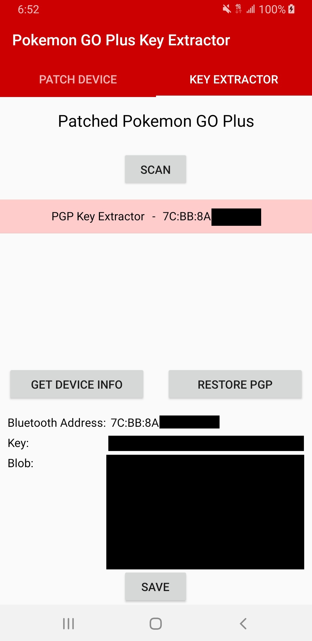
Figure 12: Successfully reading the device/blob key from a custom SUOTA Client
Risks
The valid flag is very important in verifying that the client sent the image in its entirety and that the image's integrity is intact. Because of the importance of this field, there are inherit risks by patching the valid flag. The biggest risk is if the SUOTA CRC between the client and device do not match. If this happens, I suspect that the image will still be skipped by the bootloader, even if the valid flag is correct, because the image header CRC field will not match the image CRC. However, I will not rule out the possibility that the device may brick after failing to perform a modified SUOTA. If you do end up using my software or building your own from source. YOU ACCEPT THE RISKS AND I AM NOT LIABLE FOR ANY BRICKED DEVICES. If you do not want to risk your device, you can wait until the software has been thoroughly tested by other fellow trainers. With that being said, I have successfully extracted 3 different device/blobs keys using two phones. Two of them were from legitimate PGPs and one was from a Chinese clone. The phones I used were Oneplus 5 and a Samsung Galaxy S8+.
Conclusion
This concludes my article, I hope that you found it informative. I look forward to see what the open source community will create now that all the software is free and open source. I have passionately worked on this project for the past 10 months and have learned a lot along the way. I'll feel a sense of pride and accomplishment if I get to meet fellow trainers with custom devices on community day! I would like to give a big thanks to Yohanes for all of his help, please check out his blog If you haven't done so yet. Thank you for reading!
